The GeForce 6 Series (codename NV40) is Nvidia's sixth generation of GeForce graphic processing units. Launched on April 14, 2004, the GeForce 6 family introduced PureVideo post-processing for video, SLI technology, and Shader Model 3.0 support (compliant with Microsoft DirectX 9.0c specification and OpenGL 2.0).
| Nvidia GeForce 6 Series | |
|---|---|
| Codename(s) | NV40, NV41, NV42, NV43, NV44, NV45 |
| Release date | April 2004 - 2005 |
| Entry-level GPU | 6100 (IGP), 6150 (IGP), 6200, 6500 |
| Mid-Range GPU | 6600 |
| High-end GPU | 6800 |
| Direct3D and Shader version | D3D 9.0c Shader Model 3.0 |
Contents
[hide]- 1 GeForce 6 Series features
- 2 GeForce 6800 Series
- 3 GeForce 6600 Series
- 4 GeForce 6500
- 5 GeForce 6200
- 6 GeForce 6200 TurboCache / AGP
- 7 GeForce 6100 and 6150 series
- 8 IntelliSample 4.0 and the GeForce 6 GPUs
- 9 See also
- 10 Notes and references
- 11 External links
- 11.1 Reviews
GeForce 6 Series features
SLI
See also: Scalable Link InterfaceThe Scalable Link Interface (SLI) allows two GeForce 6 cards of the same type to be connected in tandem. The driver software balances the workload to the chips. SLI-capability is limited to select members of the GeForce 6 family; 6500 and above. SLI is only available when using the PCI-Express bus.
 nVidia NV43 AGP (Geforce 6600GT)
Nvidia PureVideo Technology
Nvidia PureVideo technology is the combination of a dedicated video processing core and software which decodes H.264, VC-1, WMV, and MPEG-2 videos with reduced CPU utilization.
Shader Model 3.0
While ATI was the first to deliver Shader Model 2.0 capability to the retail market, Nvidia was the first to deliver Shader Model 3.0 (SM3) capability. SM3 extends SM2 in a number of ways: standard FP32 (32-bit floating-point) precision, dynamic branching, increased efficiency and longer shader lengths are the main additions. Shader Model 3.0 was quickly adopted by game developers because it was quite simple to convert existing shaders coded with SM 2.0/2.0A/2.0B to version 3.0, and it offered noticeable performance improvements across the entire GeForce 6 line.
Caveats
There are reports of incompatibility between GeForce 6 series cards and some wide aspect ratio LCD panels when connected through DVI[citation needed]. PureVideo functionality varies by model, with some models lacking WMV9 and/or H.264 acceleration.[1]
In addition, motherboards with some VIA and SIS chipsets and an AMD Athlon XP processor seemingly have compatibility problems with the GeForce 6600 and 6800 GPUs. Problems that have been known to arise are freezing, artifacts, reboots, and other issues that make gaming and use of 3D applications almost impossible. These problems seem to happen only on Direct3D based applications and do not affect OpenGL.[2]
Geforce 6 Series comparison
Here is how the released versions of the "GeForce 6" series family compare to Nvidia's previous flagship GPU, the GeForce FX 5950 Ultra, in addition to the comparable units of ATI's newly released for the time Radeon X800 and X850 Series:
GeForce FX 5950 Ultra GeForce 6200 TC-32 GeForce 6600 GT GeForce 6800 Ultra ATI Radeon X800 XT PE ATI Radeon X850 XT PE Transistor count 135 million 77 million 146 million 222 million 160 million 160 million Manufacturing process 0.13 µm 0.11 µm 0.11 µm 0.13 µm 0.13 µm low-k 0.13 µm low-k Die Area (mm²) ~200 110 156 288 288 297 Core clock speed (MHz) 475 350 500 400 520 540 Number of pixel shader processors 4 4 8 16 16 16 Number of pixel pipes 4 4 8 16 16 16 Number of texturing units 8(16*) 4 8 16 16 16 Number of vertex pipelines 3* 3 3 6 6 6 Peak pixel fill rate (theoretical) 1.9 Gigapixel/s 700 Megapixel/s 2.0 Gigapixel/s 6.4 Gigapixel/s 8.32 Gigapixel/s 8.64 Gigapixel/s Peak texture fill rate (theoretical) 3.8 Gigatexel/s 1.4 Gigatexel/s 4.0 Gigatexel/s 6.4 Gigatexel/s 8.32 Gigatexel/s 8.64 Gigatexel/s Memory interface 256-bit 64-bit 128-bit 256-bit 256-bit 256-bit Memory clock speed 950 MHz DDR 700 MHz DDR 1.0 GHz GDDR3 1.1 GHz GDDR3 1.12 GHz GDDR3 1.18 GHz GDDR3 Peak memory bandwidth (GB/s) 30.4 5.6 16.0 35.2 35.84 37.76 (*) GeForce FX series has an Array based Vertex Shader.
GeForce 6800 Series
The first family in the GeForce 6 product-line, the 6800 series catered to the high-performance gaming market. As the very first GeForce 6 model, the 16 pixel pipeline GeForce 6800 Ultra (NV40) was 2 to 2.5 times faster than Nvidia's previous top-line product (the GeForce FX 5950 Ultra), packed four times the number of pixel pipelines, twice the number of texture units and added a much improved pixel-shader architecture. Yet, the 6800 Ultra was fabricated on the same (IBM) 130 nanometer process node as the FX 5950, and it consumed slightly less power.
Early benchmarks put the 6800 series at a disadvantage when compared to similarly priced ATI cards. Newer drivers have improved performance on both companies' products. Against the ATI's Radeon X800XT PE, its direct competitor, the 6800 Ultra performed comparably in most synthetic and game benchmarks, with each card showing its individual strengths in different gaming applications. Nvidia's part is strong in many applications programmed for OpenGL (a traditional strength of Nvidia), while ATI leads in many Direct3D applications. Thus, it is now generally accepted that the GeForce 6800 Ultra is similar in performance to the Radeon X800 XT, and that the GeForce 6800 GT generally performs better than the Radeon X800 Pro.
In the view of many, the 6800 Ultra gave Nvidia a performance boost it had not seen since the early days of the GeForce product-line. In the aftermath of the GeForce FX series (which could only offer competitive performance in OpenGL applications), the 6800 restored faith in Nvidia's ability to deliver a competitive product. This was quite important, as the 6800 Ultra made a strong positive impression on a skeptical market, helping Nvidia regain mindshare it had lost in the aftermath of the GeForce FX.
Like all of Nvidia's GPUs up until 2004, initial 6800 members were designed for the AGP bus. Nvidia added support for the PCI Express (PCIe) bus in later GeForce 6 products, usually by use of an AGP-PCIe bridge chip. In the case of the 6800GT and 6800Ultra, Nvidia developed a variant of the NV40 chip called the NV45. The NV45 shares the same die core as the NV40, but embeds an AGP-PCIe bridge on the chip's package. (Internally, the NV45 is an AGP NV40 with added bus-translation logic, to permit interfacing with a PCIe motherboard. Externally, the NV45 is a single chip with two separate silicon dies clearly visible on the top.)
The use of an AGP-PCIe bridge chip initially led to fears that natively-AGP GPUs would not be able to take advantage of the additional bandwidth offered by PCIe and would therefore be at a disadvantage relative to native PCIe chips. However, benchmarking reveals that even AGP 4x is fast enough that most contemporary games do not improve significantly in performance when switched to AGP 8x, rendering the further bandwidth increase provided by PCIe largely superfluous. Additionally, Nvidia's on-board implementations of AGP are clocked at AGP 12x or 16x, providing bandwidth comparable to PCIe for the rare situations when this bandwidth is actually necessary.
The use of a bridge chip allowed Nvidia to release a full complement of PCIe graphics cards without having to redesign them for the PCIe interface. Later, when Nvidia's GPUs were designed to use PCIe natively, the bidirectional bridge chip allowed them to be used in AGP cards. ATI, initially a critic of the bridge chip, eventually designed a similar mechanism for their own cards.
Nvidia's professional Quadro line contains members drawn from the 6800 series: Quadro FX 4000 (AGP) and the Quadro FX 3400, 4400 and 4400g (both PCI Express). The 6800 series was also incorporated into laptops with the GeForce Go 6800 and Go 6800 Ultra GPUs.
PureVideo and the AGP GeForce 6800
PureVideo expanded the level of multimedia-video support from decoding of MPEG-2 video to decoding of more advanced codecs (MPEG-4, WMV9), enhanced post-processing (advanced de-interlacing), and limited acceleration for encoding. But perhaps ironically, the first GeForce product(s) to offer PureVideo, the AGP GeForce 6800/GT/Ultra, failed to support all of PureVideo's advertised features.
Media player software (WMP9) with support for WMV-acceleration did not become available until several months after the 6800's introduction. User and web reports showed little if any difference between PureVideo enabled GeForces and non-Purevideo cards. The prolonged public silence of Nvidia, after promising updated drivers, and test benchmarks gathered by users led the user community to conclude that the WMV9 decoder component of the AGP 6800's PureVideo unit is either non-functional or intentionally disabled.
In late 2005, an update to Nvidia's website finally confirmed what had long been suspected by the user community: WMV-acceleration is not available on the AGP 6800. Of course, today's standard computers are fast enough to play WMV9 video and other sophisticated codecs like MPEG-4, H.264 or Theora without hardware acceleration.
GeForce 6 series general features
- 4, 8, 12, or 16 pixel-pipeline GPU architecture
- Up to 8x more shading performance compared to the previous generation
- CineFX 3.0 engine - DirectX 9 Shader Model 3.0 support
- On Chip Video processor (PureVideo)
- Full MPEG-2 encoding and decoding at GPU level (PureVideo)
- Advanced Adaptive De-Interlacing (PureVideo)
- DDR and GDDR-3 memory on a 256-bit wide Memory interface
- UltraShadow II technology - 3x to 4x faster than NV35 (GeForce FX 5900)
- High Precision Dynamic Range (HPDR) technology
- 128-bit studio precision through the entire pipeline - Floating-point 32-bit color precision
- IntelliSample 4.0 Technology - 16x Anisotropic Filtering, Rotating Grid Antialiasing and Transparency Antialiasing (see here)
- Max Resolution is 2048x1536@85 Hz
- Video Scaling and Filtering - HQ filtering techniques up to HDTV resolutions
- Integrated TV Encoder - TV-output up to 1024x768 resolutions
- OpenGL 2.0 Optimizations and support
- DVC 3.0 (Digital Vibrance Control)
- Dual 400 MHz RAMDACs which support QXGA displays up to 2048x1536 @ 85 Hz
- Dual DVI on select members (Depending on the Card Manufacturer.)
6800 chipset table
Board Name Core Type Core
(MHz)Memory
(MHz)Pipeline
ConfigVertex
ProcessorsMemory
Interface6800 Ultra NV40/NV45 400 1100 16 6 256-bit 6800 GT NV40/NV45 350 1000 16 6 256-bit 6800 GS NV40/NV42 350/425 1000 12 5 256-bit 6800 GTO NV40/NV45 350 900 12 5 256-bit 6800 NV40/NV41
NV42325 700/600 12 5 256-bit 6800 Go NV41M 300 600 12 5 256-bit 6800 Go Ultra NV41M(0.13u)/NV42M(0.11u) 450 1100 12 5 256-bit 6800 XT NV40/NV41/NV42 325/350/? 700/1000+ 8 4 128/256-bit 6800 XE NV40 275/300/325 533/700 8 3 128-bit 6800 LE NV40 300 700 8 4 256-bit - The GeForce 6800 GS is cheaper to manufacture and has a lower MSRP than the GeForce 6800 GT because it has fewer pipelines and a smaller process (110 vs 130 nm), but performance is similar because it has a faster core clock. The AGP version, however, uses the original NV40 chip and 6800 GT circuit board and may be capable of re-activating the inactive pixel and vertex pipes. Unfortunately, the PCI Express version lacks them entirely, precluding such modifications.
- The 6800 GTO (which was produced only as an OEM card) contains four masked pixel pipelines and one masked vertex shader, which are potentially unlockable.
- The GeForce 6800 is often unofficially called the "GeForce 6800 Vanilla" or the "GeForce 6800 NU" (for Non-Ultra) to distinguish it from the other models. Recent PCIe variants have the NV41 (IBM 0.13 micrometre) or NV42 (TSMC 0.11 micrometre) cores, which are native PCIe implementations and do not have an integrated AGP bridge chip. The AGP version of the video card contains four masked pixel pipelines and one masked vertex shader, which are potentially unlockable through software mods. PCI-Express 6800 cards are incapable of such modifications, because the extra pixel pipelines and vertex buffers are nonexistent.
- The 6800 XT varies greatly depending on manufacturer. It is produced on three cores (NV40/NV41/NV42), four memory configurations (128MB DDR, 256 MB DDR, 128 MB GDDR3, and 256 MB GDDR3), and has clock speeds ranging from 300-425 (core) and 600-1000 (memory). 6800 XT cards based on the NV40 core contain eight masked pixel pipelines and two masked vertex shaders, and those based on the NV42 core contain four masked pipelines and one masked shader (for some reason, the NV42 cards are almost never unlockable. It is speculated that the pipelines are being laser-cut).
- The 6800 LE contains eight masked pixel pipelines and two masked vertex shaders, which are potentially unlockable.
GeForce 6600 Series
The GeForce 6600 (NV43) was officially launched on August 12, 2004, several months after the launch of the 6800 Ultra. With half the pixel pipelines and vertex shaders of the 6800 GT, and a smaller 128-bit memory bus, the lower-performance and lower-cost 6600 is the mainstream product of the GeForce 6 series. The 6600 series retains the core rendering features of the 6800 series, including SLI. Equipped with fewer rendering units, the 6600 series processes pixel data at a slower rate than the more powerful 6800 series. However, the reduction in hardware resources, and migration to TSMC's 110 nm manufacturing process (versus the 6800's 130 nm process), make the 6600 both less expensive for Nvidia to manufacture and less expensive for customers to purchase.
Their 6600 series currently has three variants: the GeForce 6600LE, the 6600, and the 6600GT (in order from slowest to fastest.) The 6600 GT performs quite a bit better than the GeForce FX 5950 Ultra or Radeon 9800 XT, with the 6600 GT scoring around 8000 in 3DMark03, while the GeForce FX 5950 Ultra scored around 6000, and it is also much cheaper. Notably, the 6600 GT offered identical performance to ATI's high-end X800 PRO graphics card with drivers previous December 2004, when running the popular game Doom 3 (afterwards ATI optimized their drivers and was able to distance itself slightly from the 6600GT). It was also about as fast as the higher-end GeForce 6800 when running games without anti-aliasing in most scenarios.
At introduction, the 6600 family was only available in PCI Express form. AGP models became available roughly a month later, through the use of Nvidia's AGP-PCIe bridge chip. A majority of the AGP GeForce 6600GTs have their memory clocked at 900 MHz, which is 100 MHz below the PCI-E card, on which the memory operates at 1000 MHz. This can contribute to a performance decline when playing certain games. However, many times it is possible to "overclock" the memory to its nominal frequency of 1000 MHz.
6600 chipset table
Board Name Core Type Core
(MHz)Memory
(MHz)Pipeline
ConfigVertex
ProcessorsMemory
Interface6700 XL NV43 525 1100 8 3 128-bit 6600 GT GDDR3 NV43 500 900/1000 8 3 128-bit 6610 XL NV43 400 800 8 3 128-bit 6600 DDR2 NV43 350 800 8 3 128-bit 6600 NV43 300 500/550 8 3 128-bit 6600 LE NV43 300 500 4 3 128-bit 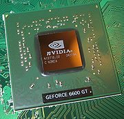 GeForce 6600GT GPU chip
Other data for PCI Express based cards:
- Memory Interface: 128-bit
- Memory Bandwidth: 16.0 GB/s.
- Fill Rate (pixels/s.): 4.0 billion
- Vertices per Second: 375 million
- Memory Data Rate: 1000 MHz
- Pixels per Clock (peak): 8
- RAMDACs: 400 MHz
Other data for AGP based cards:
- Memory Interface: 128-bit
- Memory Bandwidth: 14.4 GB/s.
- Fill Rate (pixels/s.): 4.0 billion
- Vertices per Second: 375 million
- Memory Data Rate: 900 MHz
- Pixels per Clock (peak): 8
- RAMDACs400 MH
GeForce 6500
- Core Clock: 450 MHz
- Memory Clock: 700 MHz
- Pixel Pipelines: 4
- Number of ROPs: 2
- Vertex Processors: 3
- Memory: 128MB/256MB DDR on a 64-bit interface
- Fill Rate (pixels/s): 1.6 billion
- Vertices per Second: 300 million
- Effective Memory Bandwidth(GB/s): 13.44
GeForce 6200
- Core Clock: 300 MHz
- Memory Clock: 550 MHz
- Pixel Pipelines: 4
- Vertex Processors: 3
- Memory: 128 MB/256 MB/512 MB [3] DDR on a 64-bit/128-bit interface
GeForce 6200 PCI-Express (NV44) TurboCache
- Core Clock: 350 MHz
- Memory Clock: 700 MHz
- Pixel Pipelines: 4
- Number of ROPs: 2
- Vertex Processors: 3
- Memory: 16 MiB/32 MiB/64 MiB/128 MiB DDR on a 32-bit/64-bit/128-bit interface
- GeForce 6200 w/ TurboCache supporting 128 MiB, including 16 MiB of local TurboCache (32-bit)
- GeForce 6200 w/ TurboCache supporting 128 MiB, including 32 MiB of local TurboCache (64-bit)
- GeForce 6200 w/ TurboCache supporting 256 MiB, including 64 MiB of local TurboCache (64-bit)
- GeForce 6200 w/ TurboCache supporting 256 MiB, including 128 MiB of local TurboCache (128-bit)
GeForce 6200 AGP (NV44a) without TurboCache
- Core Clock: 350 MHz
- Memory Clock: 500 MHz
- Pixel Pipelines: 4
- Number of ROPs: 2
- Vertex Processors: 3
- Memory: 128-256 MB DDR on a 64-bit interface
GeForce 6200 AGP (NV44a2) without TurboCache
- Core Clock: 350 MHz
- Memory Clock: 540 MHz
- Pixel Pipelines: 4
- Vertex Processors: 3
- Memory: 128 MB/512 MB DDR2 with a 128-bit/64-bit interface
- Cooling: Passive heatsink
(Only PNY is known to manufacture this card, which appears to be discontinued.) (XFX manufactured a 6200A AGP with 512MB of ram with a 64 bit interface)
GeForce 6200 AGP (NV44a) without TurboCache
- Core Clock: 350 MHz
- Memory Clock: 532 MHz
- Pixel Pipelines: 4
- Vertex Processors: 3
- Memory: 256 MB DDR2 BGA on a 64-bit interface
GeForce 6100
- Manufacturing process: 90 nm
- Core Clock: 425 MHz
- Vertex Processors: 1
- Pixel Pipelines: 2
- Shader Model: 3
- DirectX support: v9
- Video playback acceleration: SD video acceleration (HD video acceleration not supported)
- Outputs: VGA only
- Memory: Shared DDR/DDR2 (socket 939/AM2) system memory (selectable through BIOS - usually 32/64/128/256 MB)
GeForce 6150
- Manufacturing process: 90 nm
- Core clock: 475 MHz[5]
- Vertex processors: 1
- Pixel pipelines: 2
- Shader model: 3
- DirectX support: v9
- Video playback acceleration: HD video acceleration
- Outputs: VGA, DVI, Video
- Memory: Shared DDR2 (socket 939/AM2) system memory (selectable through BIOS - usually 32/64/128/256 MB)
GeForce 6150SE
GeForce 6150SE is new single-chip version of the nVidia GeForce 6100, MCP61 (also known as C61). The MCP61 uses less power than the original C51 2-chip version of 6100 and its onboard video outperforms the 6150 in many 3D benchmarks even despite lower core frequency (425 MHz) because of added hardware Z-culling.
MCP61 introduced a bug in the SATA NCQ implementation. In detail, nvidia employees have disabled NCQ operations under Linux[1]
- Manufacturing process: 90 nm
- Core Clock: 425 MHz
- Vertex Processors: 1
- Pixel Pipelines: 2
- Shader Model: 3
- DirectX support: v9
- 11.1 Reviews


0 comments:
Post a Comment